Hybrid nanostructure mid-wave infrared harsh environment compatible sensors for Industry applications (HybNanoSens)
Polish-Singaporean Joint Research
NCBR POL-SINIV/1/2018
Smart monitoring needs uncooled high sensitivity and low-power consumption sensors to fast respond external stimulus. Middle wavelength infrared (MWIR) photon-type sensors capable of room temperature operation can best serve this purpose in the atmosphere window of 3-5 µm. However, currently available products based on HgCdTe (MCT), InSb and PbSe suffer from expensive refrigeration and high power dissipation and they cannot work well at room temperature due to the intrinsic nature of the sensing materials and device structures. In our view, the only way to break the bottleneck is to integrate the advanced nanotechnology and enhancement technique with the sensing devices
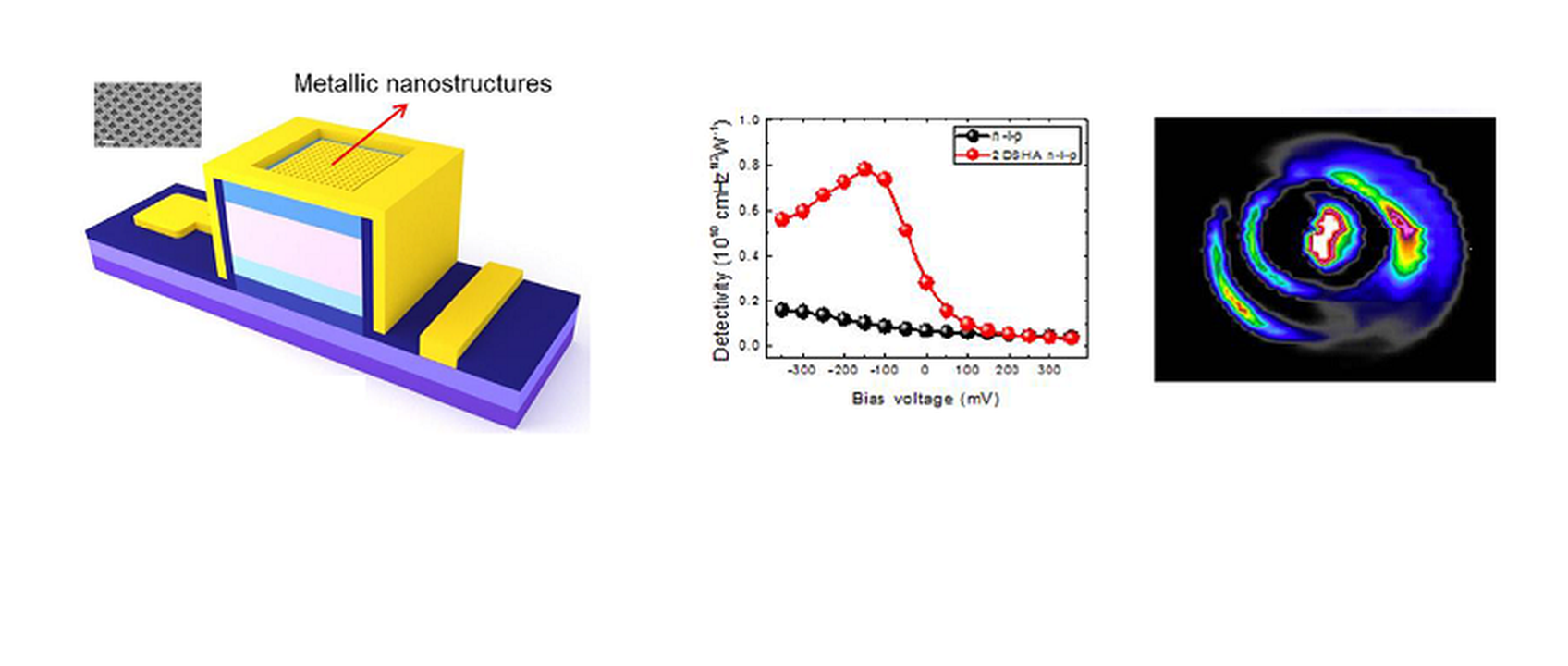
In this project, we will develop room temperature operation, zero bias, high sensitivity and harsh environment compatible sensors by integrating a specially designed InAsSb based heterojunction p-i-n photodiode with novel hybrid nanostructures. The heterojunction p-i-n photodiode contains well selected wide gap barrier layers to reduce dark current by blocking the conduction carriers, and enhance response speed by adjusting the dimension and doping concentration in the barrier layers. The hybrid nanostructures are the combination of photonic crystal slab (PhCS) and metallic hole array (MHA). The former is used to significantly reduce reflection of incident photons and confine the transmitted photons for better absorption, while the latter is to convert photons into surface plasmons, which significantly enhances quantum efficiency. The high sensitivity, fast response speed, zero power consumption (no bias) and room temperature (no cooling) sensor can work as a single device. It can also be easily extended to one or two dimensional arrays for different industry applications by combining a solar cell biased amplifier or read-out circuit.
The project involves both theoretical and experimental research. The former includes band structure of the InAsSb based heterojunction, design, simulation and optimization of hybrid PhCS and MHA. The latter involves device growth, fabrication, integration and characterization. The device can be grown with molecular beam epitaxy and fabricated with our clean room facilities, while the hybrid nanostructures can be fabricated by electron beam lithography and our newly developed technique.
The project dealing with integration of reliable semiconductor, different nanostructures, and novel design, will open a new avenue for high performance novel photonic devices and systems.